Projects: CPLD-based vintage 7-segment display controller
January 6, 2025
I decided to finally publish this project. Not because it’s a well-done, thought-out and tested project - quite the opposite, actually. But I finally found, after 2.5 years, a design error that eluded me. I decided I will fix this and describe how and why this project even came into existence.
In the beginning, there were USSR displays…
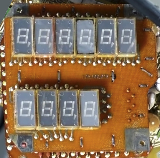
Quite some time ago (3 years I think) I received a bunch of soviet-era displays that had unusual construction - I cannot reference any part number for them, all I know is that they look identical to those Ken Shirrff presented some time ago on his blog:

I got quite a lot of them, so I decided that I will do something with them. At that time I also was interested in VHDL language and FPGAs, so I thought that I could maybe design something that would allow me to use those parts and write something more practical in VHDL. Of course, FPGAs are no easy feat - they have big packages with multiple power rails, often external clock and many more. So, I started looking at something simpler, and found that Xilinx (today AMD) produced a series of quite simple CPLDs that were still supported by ISE. They had 5V-tolerant pins (more on that later…), contained memory to store the bitstream and could be programmed using JTAG with ease. So I bought some chips and started experimenting.
OK, so what’s the plan?
First, I wanted to verify how to actually drive the displays. At this point, I wasn’t even sure if they are in common-cathode or common-anode configuration. So I got my power supply and got three important results:
- First, those displays are dim. They can chew up to 20mA per segment and still give so little light that in daylight conditions the segments are barely visible.
- Second, most of those displays were damaged. And in a interesting way - it seems like desoldering process damaged bonding between package pin and LED inside. Fortunately, just enough modules were fully working that I still was determined to continue.
- Third, pinout is actually compatible with more available
MAN72Adisplays, neat!
8 segments (dot also counts) * 20mA per segment = 160mA
There are not that many controllers that can handle this much current, and
this CPLD was not even close. So after testing various drivers and ideas,
I settled on SN74LS47 chip. According to notes I’ve left 2 years ago, I
also tested CD74HC4543 and considered MC14543B, 74HC42. Those chips are BCD to
7-segment display drivers. Having a separate chip for each display greatly reduced
complexity of the project, as the design wouldn’t require any clock to work. As
for dots, I just controlled them using one transistor separately.
I had all I needed, so I started digging into Xilinx documentation (excellent by
the way) to find all the information and requirements for the schematic. That’s
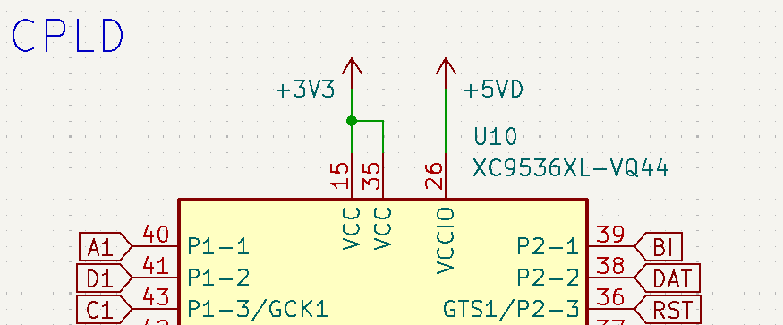
where I made a severe mistake - I thought that 5V-compatible IO meant that you can have
5V for VCCIO. So I carefully designed circuit in a way that ensured that no 5V
would be present until 3.3V line from LDO won’t be ready. I also added NE555, just
in case.
How can someone like working with ISE?
I don’t know, I didn’t have to! When I was starting my journey with VHDL, I discovered a wonderful tool called GHDL Language server for VS Code - to this day I consider this the best helper for VHDL language. Instant error messages with useful information, helpful templates, great auto-completion. For this kind of languages, it’s hard to get anything better, as most tools are just slow and unresponsive most of the time (looking at you, Vivado…).
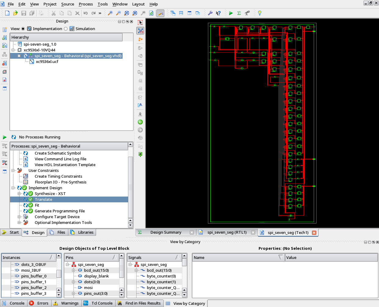
But, this is just a setup for a text editor, not for whole development cycle! For this I used FuseSoC to run ISE for me. At that time documentation for this tool was sparse, but sufficient to get things going. I managed to prepare target for simulation using GHDL and synthesis using ISE tools. I think this project really shines in comparison to other tools I know from other languages. It manages to create a simple interface to many wildly different environments from different manufacturers that are not only closed-source, but often not available for download without license or NDA. I really like the way this tool solves this problem, as it doesn’t give you much freedom on how the project has to be structured. Of course, it comes with a big downside - no vendor tools for generating wrappers or connections between different IPs. I don’t consider this as a problem, as those tools are known to be problematic and buggy. You cannot escape them when you are planning to use chips like Zynq, where generating correct bindings is required. Still, the neat thing about FuseSoC is the fact that you can still use vendor tools as it also will generate vendor project (in my case ISE) so I can still look into Schematic viewer, timing analysis and others:

There are a couple of really neat application notes for those chips, like UG445 or XAPP784 that helped tremendously.
There is now only one puzzle piece missing - programming of those CPLDs. As I didn’t
want to buy a dedicated programmer, I decided to use DirtyJTAG
to program it. I had many problems with generating required .svf file, but
fortunately iMPACT tool also has batch mode that works.
Why is this chip getting so hot?
I managed to prepare working firmware and bistream, and I was able to run displays,
but for some reason main CPLD was running really hot. The reason was of course
the fact that I powered VCCIO from 5V instead of 3.3V. Mistakes happen, but this
one eluded me for way too long. Now I know that reading Absolute Maximum Ratings
section is a must, and the fact that something is 5V-compatible can just mean “I can
withstand 5V and not be damaged” - big difference. I spent way too much time searching
for answers, trying different configurations, searching trough datasheets…


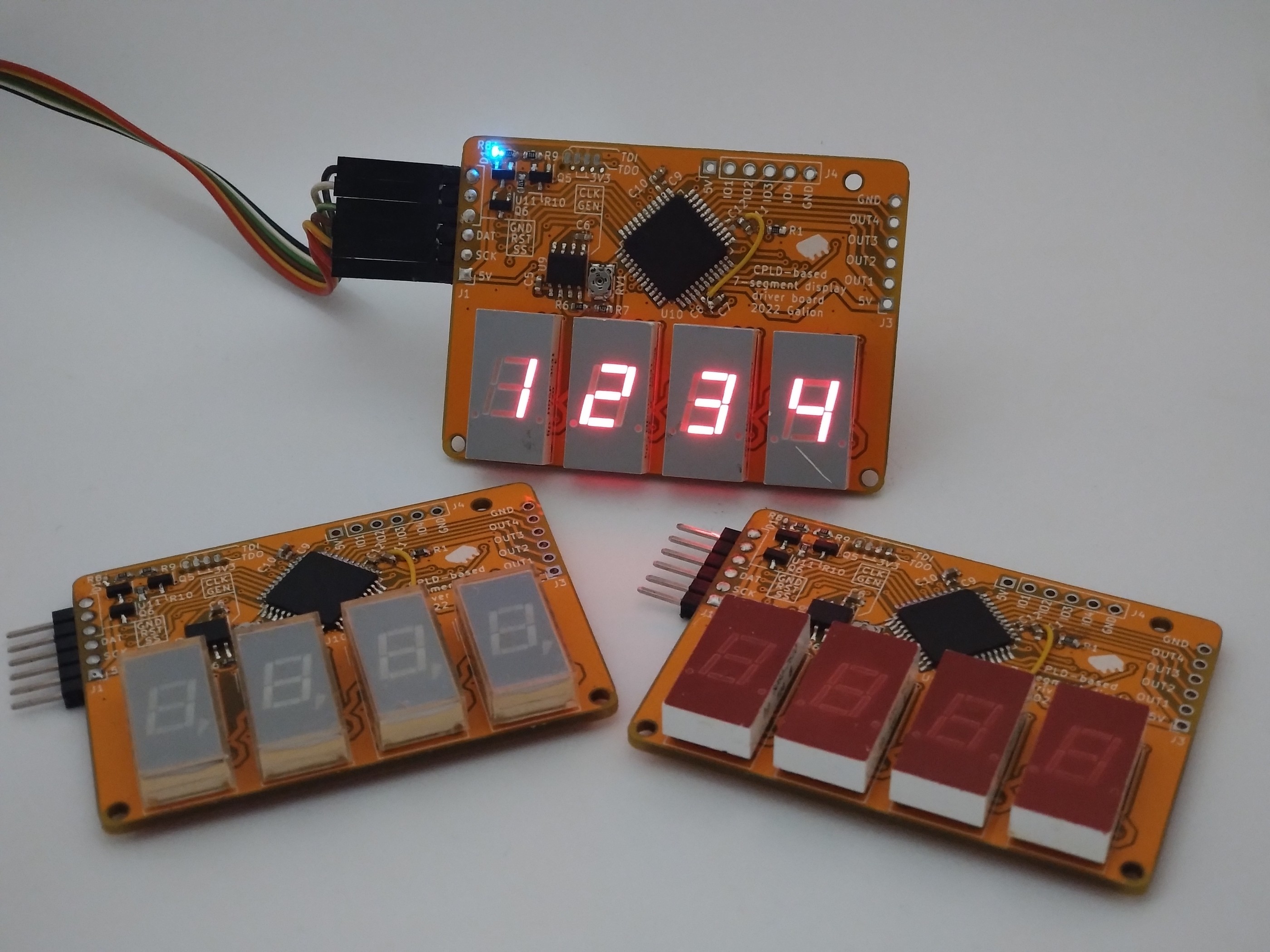
Fortunately, nowadays, after I forgot about the details, I could look into it with clear head to immediately find the mistake I made. I just added a bodge wire and fixed the problem.
I’ve also prepared 2 more boards to see how other displays (from HP this time) would work. The difference is staggering - with 20mA per segment you can actually see the contents even in daylight.

Some conclusions
Not many this time - the hard part of designing things for me, is to be consistent. Being able to follow the process is not possible if there is no written procedure. That’s why I now use my own design checklist, mostly based on those available online. And most importantly - for me it’s better to actually focus on one part of the project, finish, check and perfect that and only then go to the next schematic page, circuit, or layout part. There is just too much stuff to do at once, and my short-term memory doesn’t help at all.